

Integrated Circuit Forensics
Integrated circuits are at the center of failures, disputes, and security concerns that span product liability, patent litigation, insurance claims, and national supply chain security. GDF applies non-destructive and destructive analytical techniques to characterize IC failures, authenticate components, detect hardware modifications, and produce expert findings that meet the standards required in technical litigation and regulatory proceedings.
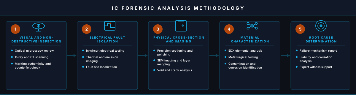
The Role of IC Forensics in Litigation and Technical Disputes
Integrated circuits are the foundational components of every electronic system, from consumer devices and medical equipment to automotive control modules and industrial machinery. When an IC fails, behaves unexpectedly, or is suspected of being counterfeit or hardware-modified, the consequences extend far beyond the component itself. Equipment fails. Systems become unreliable. People are injured. Contracts are disputed. Insurance claims are filed. Patents are litigated.
IC forensic analysis provides the physical, electrical, and material evidence needed to answer the technical questions underlying these disputes. Is the failure attributable to a manufacturing defect, to an operating condition that exceeded the device's rated specifications, to electrostatic discharge, or to a design error? Is the component authentic, or has it been remarked, refurbished, or counterfeited? Does the competitor's chip design embody the structural features claimed in the patent at issue? Is the hardware modification alleged in the complaint physically present in the device?
These questions require specialized equipment, documented analytical procedures, and examiners who can explain complex semiconductor physics to attorneys, judges, and juries. GDF's IC forensics practice combines laboratory capability with litigation support expertise, producing findings that are technically accurate, procedurally defensible, and presented in terms that non-technical decision-makers can follow. For matters where IC forensics intersects with broader embedded system concerns, GDF's embedded systems forensics team can extend the analysis to firmware, memory, and device-level evidence.
Non-Destructive Analysis Techniques
GDF applies non-destructive analysis as the first phase of every IC examination, preserving the physical state of the component while characterizing its structure, materials, and condition. Non-destructive findings document the baseline state of the component and frequently resolve the question at issue without requiring destructive preparation.
X-Ray Imaging
X-ray radiography provides a two-dimensional image of the internal structure of a packaged IC without any physical preparation. X-ray imaging reveals bond wire routing and geometry, die size and placement relative to the package, solder joint formation and void content in BGA packages, lead frame configuration, and internal package features including die attach layer condition and delamination. In counterfeit detection, X-ray images are compared to authenticated reference components to identify discrepancies in internal structure that indicate remarking, die substitution, or repackaging.
3D X-ray computed tomography (CT) extends this capability, providing volumetric imaging of complex packages including multi-die stacks, system-in-package modules, and through-silicon via (TSV) assemblies where two-dimensional X-ray cannot resolve all features of interest. GDF uses high-resolution X-ray systems capable of sub-micron voxel resolution for detailed structural characterization.
Acoustic Microscopy (CSAM)
C-mode scanning acoustic microscopy (CSAM) uses focused ultrasound to image internal features of packaged ICs based on acoustic reflectivity. CSAM is particularly sensitive to delamination, voids, and cracks at interfaces within the package: between the die and die attach layer, between the die attach layer and lead frame, and between mold compound and die surface or internal structures. These defects are not visible in X-ray imaging but are directly relevant to reliability, failure analysis, and authentication.
In failure analysis, CSAM identifies delamination that preceded or resulted from thermal stress failures, package cracking that contributed to moisture ingress, and voiding in thermal interface materials that caused localized overheating. In counterfeit detection, CSAM reveals package rework artifacts including die removal and reinstallation that leave characteristic acoustic signatures at package interfaces.
Scanning Electron Microscopy (SEM) and Optical Inspection
SEM provides high-resolution surface imaging of IC dies, bond wires, package surfaces, and cross-sections prepared for analysis. GDF uses SEM for surface contamination characterization, corrosion documentation, bond wire morphology analysis, and defect imaging on die surfaces exposed through decapsulation. Energy-dispersive X-ray spectroscopy (EDS) performed in conjunction with SEM provides elemental composition data for material identification: characterizing bond wire composition (gold vs. copper vs. aluminum), identifying contaminants, and verifying metallization layer compositions.
High-magnification optical inspection under calibrated microscopes provides surface characterization at resolutions appropriate for package marking inspection, lead finish condition assessment, and preliminary die surface review. GDF's optical inspection procedures follow JEDEC and ASTM standards applicable to visual inspection of electronic components and produce photographic documentation at multiple magnifications for inclusion in expert reports.
Destructive Analysis Techniques
When non-destructive analysis does not provide sufficient information to address the question at issue, GDF proceeds to destructive analysis with documented consent from the submitting attorney or client. Because destructive analysis alters or destroys the physical evidence, all non-destructive analysis and photographic documentation are completed before any destructive preparation begins. Chain of custody is maintained throughout, with each procedural step documented in the laboratory record.
Chemical Decapsulation
Decapsulation removes the plastic mold compound covering the IC die using fuming nitric acid, hot sulfuric acid, or proprietary solvent systems, exposing the die surface for inspection and further analysis. GDF's decapsulation procedures are designed to preserve die surface features including metal interconnect layers, passivation, and bond pad condition while completely removing the encapsulant. Selective decapsulation targets specific die areas while preserving bond wire connections for post-decapsulation electrical testing.
Die surface examination after decapsulation reveals process node indicators (metal pitch, feature geometry, passivation characteristics), die markings that are not visible through the package, circuit architecture features relevant to patent comparisons, and damage signatures including electrostatic discharge (ESD) damage, latch-up, electrical overstress (EOS), and gate oxide breakdown that are not visible through other techniques.
Focused Ion Beam (FIB) Cross-Sectioning
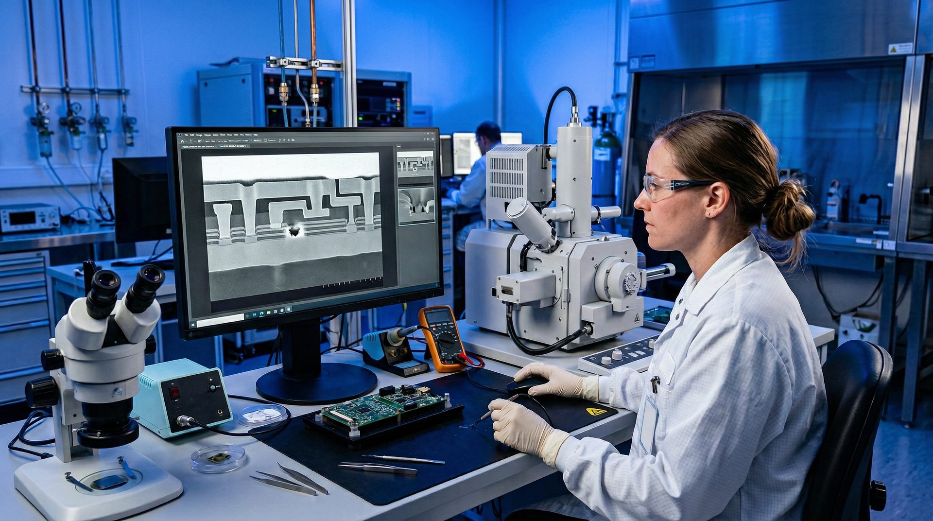
Focused ion beam processing uses a beam of gallium ions to mill precise cross-sections through IC structures at nanometer resolution. FIB cross-sections expose internal metal interconnect layers, via structures, gate oxide layers, and junction regions for imaging with SEM. This technique is essential for failure analysis at advanced process nodes where defect features are too small to resolve with other preparation methods.
FIB analysis is used to characterize gate oxide integrity failures, electromigration damage in metal interconnects, contact and via voiding, dielectric breakdown, and junction spiking. In patent litigation, FIB cross-sections document structural features including transistor geometry, interconnect architecture, and material compositions that are claimed in the patent at issue and must be present in the accused device to establish infringement.
Chip-Off Data Extraction
Chip-off extraction removes non-volatile memory dies from their packages for direct electrical readout. In IC forensics, chip-off is applied to NAND flash, NOR flash, EEPROM, and other memory types in both standalone memory packages and in embedded memory within complex ICs. The technique is used to recover stored data from damaged, locked, or encrypted devices where software-based extraction is not possible.
GDF's chip-off capabilities support forensic data recovery from automotive ECU flash memories, industrial controller firmware storage, and consumer device flash storage. For automotive and embedded systems applications, chip-off is coordinated with GDF's automobile ECU forensics and embedded systems forensics practices, which provide the firmware analysis and data interpretation expertise that transforms raw chip-off output into admissible evidence.
Electrical Fault Isolation
Electrical characterization and fault isolation techniques locate specific defects within an IC using electrical signatures, emission patterns, and timing measurements that point to physical defect sites. These techniques bridge the gap between electrical failure symptoms and physical defect location, allowing efficient targeting of subsequent physical analysis.
Photon Emission Microscopy (PEM) and EMMI
Photon emission microscopy detects weak light emission from reverse-biased junctions, gate oxide leakage sites, and hot carrier emission in metal interconnects. When the IC is biased to reproduce the failure condition, emission sites correspond to the location of the defect. EMMI (emission microscopy inspection) examines the IC in a dark, light-shielded environment using a cooled CCD or InGaAs detector sensitive to the emission wavelengths characteristic of silicon device physics.
Time-Domain Reflectometry (TDR) and EOTPR
TDR applies fast electrical pulses to package leads and analyzes reflected pulse characteristics to locate opens, shorts, and impedance discontinuities in bond wires, internal interconnects, and package substrates. Electro-optical terahertz pulse reflectometry (EOTPR) extends this capability to characterize defects in TSV structures and advanced packaging at picosecond time resolution. These techniques locate defects in three dimensions before any physical preparation begins, allowing decapsulation or FIB work to be targeted precisely at the defect site.
Lock-In Thermography (LIT) and Infrared Analysis
Lock-in thermography maps heat dissipation across the IC surface under periodic electrical excitation, revealing localized heating at defect sites including leakage current paths, partial shorts, and high-resistance contacts. Infrared thermal imaging under steady-state operation provides complementary temperature mapping for devices where lock-in excitation is not practical. Both techniques are non-destructive and occur before any physical preparation that might alter the thermal response.
Counterfeit IC Detection
The counterfeit semiconductor market is a significant problem for defense contractors, industrial equipment manufacturers, medical device companies, and anyone procuring electronic components through non-authorized distribution channels. Counterfeit ICs can be recycled parts removed from decommissioned equipment and relabeled with new date codes, inferior or non-functional components remarked with markings from premium devices, components that fail early or under stress, or, in the most serious cases, components that perform their stated function but include unauthorized hardware modifications.
GDF's counterfeit detection analysis follows the process flow defined in JEDEC JEP196 (Counterfeit Electronic Parts: Avoid, Detect, Mitigate and Dispose) and applicable ASTM standards including ASTM F1168. The analysis covers external visual inspection under microscopy, X-ray comparison against authenticated reference samples, CSAM acoustic screening for rework artifacts, decapsulation and die surface comparison, and electrical testing against manufacturer specifications.
Findings are documented with photographic evidence at each analytical stage, measurement data with reference to authentic component specifications, and a written opinion on the authenticity status of each sample examined. This documentation supports acceptance rejection decisions, contract disputes with suppliers, civil litigation against component brokers who supplied counterfeit parts, and referrals to law enforcement or customs authorities where criminal counterfeiting is indicated.
Hardware Trojan Detection
A hardware Trojan is an unauthorized modification to an IC's design or physical implementation that introduces unintended functionality: creating a covert communication channel, disabling security features under specific trigger conditions, causing malfunction or destruction of the device on command, or extracting sensitive data through side-channel emissions. Hardware Trojans are a concern in defense, intelligence, and critical infrastructure applications where components may be sourced from or processed through untrusted parties.
GDF's hardware Trojan analysis applies both physical and functional analysis techniques. Physical analysis uses SEM imaging, FIB cross-sectioning, and comparison of circuit netlist features extracted from decapsulated die images against known-good reference designs to identify unauthorized circuitry. Functional analysis uses formal verification methods, side-channel analysis (measuring power consumption, electromagnetic emissions, and timing characteristics under controlled test conditions), and penetration of security features using fault injection techniques to identify non-specified behaviors.
Hardware Trojan analysis requires reference samples of authenticated devices and, where available, design documentation. GDF works with clients to structure the analysis around the specific threat model relevant to their application, focusing the examination on the circuit areas and functional behaviors most likely to be affected by the categories of Trojan insertion relevant to the supply chain in question.
Patent Litigation Support
IC patent litigation requires forensic analysis to confirm that the structural and functional features claimed in a patent are present in an accused device, or to document their absence. This analysis is inherently physical: patent claims describing transistor architectures, interconnect structures, memory cell configurations, or process sequences must be mapped to physical features that can be documented through the analytical techniques described above.
GDF provides patent claim mapping analysis for both patent holders seeking to establish infringement and defendants seeking to establish non-infringement or design-around arguments. The analysis produces a physical feature comparison table mapping each claim element to the corresponding physical feature in the accused device, supported by SEM images, FIB cross-sections, EDS compositional data, and electrical measurements. This evidence is formatted for inclusion in expert reports under Federal Rule of Evidence 702 and Federal Rule of Civil Procedure 26.
GDF's IC forensics experts have experience testifying in federal district court proceedings on patent claims involving CMOS process technology, memory array architecture, power management IC design, and mixed-signal integrated circuit implementations. Expert report preparation, deposition preparation, and trial testimony are available as part of GDF's litigation support practice.
Product Liability and Insurance Matters
When an electronic system fails in a way that causes property damage, equipment loss, fire, or personal injury, the root cause analysis frequently points to an integrated circuit as the initiating failure. Root cause analysis must distinguish among manufacturing defects, design deficiencies, application conditions outside the device's rated specifications, and assembly errors. The answer directly determines which party in the product chain bears liability: the device manufacturer, the IC vendor, the contract assembler, or the end user.
GDF's product liability IC analysis begins with a systematic review of the failure mode and its electrical and physical manifestations, followed by a structured analytical program to characterize the failure at the physical level and compare observed failure signatures against the known failure signatures associated with each candidate cause. Gate oxide breakdown has characteristic breakdown morphology that distinguishes ESD events from electrical overstress from infant mortality failures from wear-out. Electromigration damage has characteristic void and hillock formation patterns that differ from corrosion damage or mechanical stress damage. These distinctions determine which party in the product chain bears responsibility for the failure.
For insurance claims involving electronic equipment failures, GDF provides root cause analysis that supports underwriting determinations, claim acceptance or denial decisions, and subrogation actions against responsible parties. GDF's reports in insurance matters address coverage questions directly: did the failure fall within the policy's covered causes, was it pre-existing or sudden, and did negligence or substandard components contribute to the loss.
Standards and Quality Framework
GDF's IC forensics practice operates under a quality framework that ensures the reliability and defensibility of findings:
- ISO/IEC 17025: GDF's laboratory quality management system incorporates ISO/IEC 17025 principles for testing and calibration laboratory competence, covering equipment calibration, method validation, reference material traceability, and result uncertainty quantification
- JEDEC standards: GDF applies JEDEC standards for IC failure analysis procedures, counterfeit component detection (JEP196), and failure mode documentation, ensuring compatibility with industry-standard quality systems and audit requirements
- ASTM standards: Applicable ASTM standards for electronic component testing, failure analysis, and materials characterization govern GDF's analytical procedures
- NIST SP 800-86: For matters involving IC forensics in digital evidence contexts, GDF applies NIST SP 800-86 guidance on integrating forensic techniques into incident response
- IEEE standards: IEEE 1838 and related standards for 3D IC testing inform GDF's approach to advanced packaging failure analysis
Last updated: April 16, 2026
Non-Destructive Analysis
- X-ray and 3D CT imaging
- Acoustic microscopy (CSAM) for voids and delamination
- SEM surface imaging with EDS composition
- High-magnification optical inspection
Destructive Techniques
- Chemical decapsulation and die surface analysis
- FIB cross-sectioning at nanometer resolution
- Chip-off memory data extraction
- TEM lamella preparation and analysis
Electrical Fault Isolation
- Photon emission microscopy (PEM/EMMI)
- Lock-in thermography and IR thermal analysis
- Time-domain reflectometry (TDR/EOTPR)
- Parametric and functional electrical testing
Litigation Support
- Patent claim mapping with physical evidence
- Counterfeit component authentication per JEDEC
- Product liability root cause analysis
- Expert witness testimony in federal and state courts
Request an IC Forensics Consultation
GDF works with attorneys, manufacturers, and insurers on IC failure analysis, counterfeit detection, and patent litigation support. All engagements are strictly confidential.